Mohan Majhi lays foundation stone for India’s 1st Advanced 3D Chip Packaging Unit
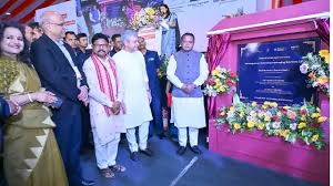
Bhubaneswar: Chief Minister Mohan Charan Majhi on Sunday laid foundation stone for the 3D Glass Solutions Inc. (3DGS)’s advanced chip packaging facility at Info Valley in Bhubaneswar in presence of Union Minister and IT minister Ashwini Vaishnaw, Electronics and IT Minister
Mukesh Mahaling and other distinguished guests.
The facility will be set up by Heterogeneous Integration Packaging Solutions, also known as 3D glass solutions. The government said the project will bring advanced chip packaging technology to India, and would help to create 2,500 jobs.
Union Minister Ashwini Vaishnaw termed the foundation laying of a semiconductor plant in Odisha is indeed a very important day, a historical day today for Odisha. It’s very important for Odisha to have a world-class, latest technology industry here. Odisha is now becoming an IT hub. It is becoming an electronics manufacturing hub. It is diversifying from metals and minerals to many new industrial bases.
The Centre had earlier approved semiconductor manufacturing units in Odisha in 2025, including projects by SiCSem Private Limited and 3D Glass Solutions Inc. (3DGS). SiCSem, in collaboration with Clas-SiC Wafer Fab Ltd., UK, will establish India’s first commercial compound semiconductor fabrication unit in Info Valley, Bhubaneswar.
SiCSem, in collaboration with Clas-SiC Wafer Fab Ltd., UK, will establish India’s first commercial compound semiconductor fabrication unit focused on Silicon Carbide (SiC) devices. The facility is expected to have an annual capacity of 60,000 wafers and a packaging capacity of 96 million units, catering to sectors such as defence, electric vehicles, railways, and renewable energy.
Meanwhile, 3DGS will set up an advanced packaging and embedded glass substrate unit. It will introduce technologies such as glass interposers and 3D heterogeneous integration modules. The unit is expected to produce 69,600 glass panel substrates and 50 million assembled units each year.
These will have applications in artificial intelligence, high-performance computing and photonics.
The Centre had approved 10 semiconductor projects nationwide, with cumulative investments exceeding Rs 1.6 lakh crore, with Odisha hosting two of them. The initiative is expected to generate over 2,000 skilled jobs and strengthen India’s ambition of building a self-reliant semiconductor ecosystem.